Operator using a digital microscope for soldering and PCB inspection

GUIDE

How to use a digital microscope for soldering and PCB inspection

Take your soldering and PCB inspections to the next level with a digital microscope. Learn how, why and the benefits here.

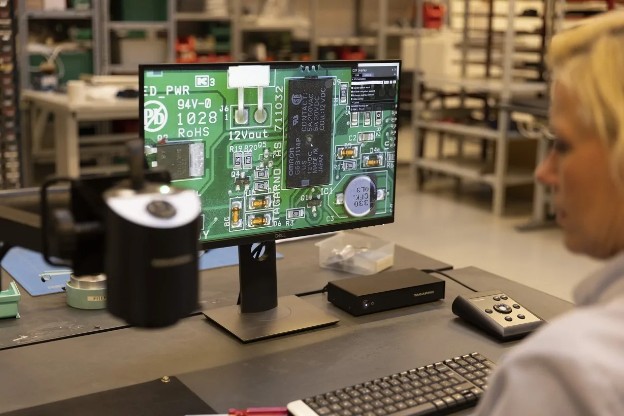
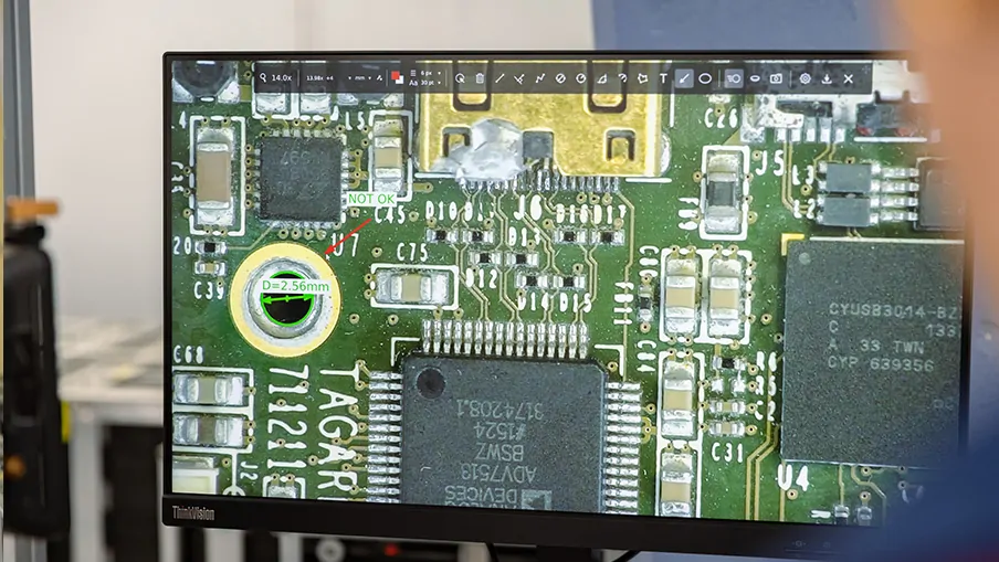
Magnification has been an integrated and crucial part of PCB production and rework for many years.

What many Electronics professionals find today, however, is that traditional magnification systems can no longer provide the required magnification levels when doing PCB inspection control or reworking faulty PCBs – nor are they equipped to capture photos and create documentation of your work in an efficient way. This sends PCB manufacturers hunting for new equipment that can do the job.

If that sounds familiar or if you’re simply curious about how to use a digital microscope for soldering and PCB inspection, this guide is the right place for you.

TAGARNO MOVE inspecting Circuit board

What to consider when choosing a digital microscope for soldering and PCB inspection

If you’re hunting for a new digital microscope for soldering and PCB inspection, it’s important that it meets certain requirements. Make sure that the digital microscope you are considering has the following features and technical specifications.

Working height

First and foremost, it’s important that there’s enough room underneath the microscope to fit the tools you’ll be using. This is referred to as working height.

Some digital microscopes can be adjusted in height which adds a lot of flexibility while others only have one height setting. Which kind you prefer is up to you.

Working area

It’s also important to consider how much space you need underneath the microscope. This will depend on the size of boards you’ll be inspection and/or reworking. For smaller boards, you don’t need much space and a microscope with a short arm will suffice. But if you’re working with bigger boards, you need a longer arm and a bigger working area to do your PCB repair.

Ergonomics

If operators are spending long hours at the microscope, it is important to create an ergonomic setup that is comfortable for them to use. Choosing an ergonomic microscope, such as a microscope with a monitor rather than an eyepiece, can reduce job-related pain for the operators which in turn will affect their productivity, reduce PCB escape rate and ultimately reduce customer claims.

Excellent images without delay

Whether you’re soldering or doing PCB inspection, it’s important with a microscope that produces high quality images without any delay between what’s happening underneath the microscope and on the monitor. If the operator experiences a delay when working with the microscope, it will not only lead to frustration but also errors during the PCB repair which of course are to be avoided.

Taking photos of your findings

With more and more companies needing to document the quality of their work, it’s important to choose a microscope where you can easily capture photos of your findings or completed work. These photos can be saved for documentation purposes or forwarded to business partners to discuss how to proceed if an issue has been identified.

Don't miss out on this free e-book

With this e-book, you'll hear directly from a customer why they chose TAGARNO's digital microscopes and how they use them today.


You'll also learn even more about the benefits of a digital microscope and how you can find the right microscope for your business.


Download free e-book
Preview of E-book concerning using a digital microscope in the Electronics industry
Download free e-book

The benefits of using a digital microscope for soldering and PCB inspection

Digital microscopes are excellent tools for soldering and PCB inspections for a variety of reasons. The first being that they meet the requirements mentioned above: Sufficient working height and working area, are ergonomically designed, produce excellent images and have easy documentation processes.

Other benefits of using a digital microscope for soldering and PCB inspections include being able to meet IPC standards and using software to perform faster and more accurate PCB inspections.

Meet IPC standards

In PCB manufacturing and assembly, it’s crucial that you meet the IPC standards. The IPC standards cover every process of PCB design, production and assembly and have become the universal standards for the electronics manufacturing industry.

When needed, the IPC standards specify the magnification power required to check the quality of your work. Using a digital microscope that produces high quality images at the required magnification is thus a prerequisite for meeting the IPC standards.

With a digital microscope, you will also be able to document that you’ve completed the inspections and that your products meet the IPC standards.

Use software for faster and more accurate inspections

Another benefit of using a digital microscope for soldering and PCB inspections is having access to software.

Below, we’ve listed the most commonly used software for PCB inspection, PCB analysis and PCB analysis. We’ll also explain how they can help you work more efficiently and accurately.

  • Measurement app

The bestselling software for PCB inspection is the Measurement app. With Measurement app, you can perform highly accurate measurements directly on the microscope. You can even use the annotation tool to highlight or comment on the completed inspection before saving it as a photo.

For easier PCB inspections going forward, the measurements themselves can also be saved as a heads-up display. This allows you to quickly verify new samples without performing a new measurement every single time.

  • Image comparison app

Another important piece of software for PCB inspection is the Image comparison app. With this app, you can use a golden sample photo as a reference during new inspections to quickly spot deviations. This makes the Image comparison a great addition to your PCB analysis processes.

  • DXF overlay app

When doing rework of a specific component, use the DXF overlay app to locate it in seconds. All you need to do is type the name of a component into the search bar and let the app find it for you. This is much faster than having to find it manually and can significantly reduce the amount of time you spend at rework stations before starting the PCB repair.

PCB manufacturer using a digital microscope for solder and digital microscope

Different Electronics processes where you can use a digital microscope

Thanks to the versatility of digital microscopes, there’s many processes within PCB manufacturing where they can add value to your business. Let’s have a look at some examples of where digital microscopes are especially useful.

Research and development

A digital microscope is an excellent tool for First article inspections (FAI) due to its high image quality and how easy it is to capture images of your work and/or issues.

With apps like Measurement app, Focus stacking app and DXF overlay app, you can enrich your captured photos with even more detail when documenting that each component has been placed as specified.

Quality assurance and quality control

With the excellent image quality and smooth live image of a digital microscope, it’s easy to check the conformal coating application, if components have been placed correctly and more.

You can also use apps like Image comparison during this process to compare your current PCB to a photo of a golden sample to quickly spot deviations, and you can use presets to save and reuse your most used settings. This eliminates the need for manual adjustment of the microscope, thus ensuring consistency across your PCB inspections and increased efficiency.

Repair and rework

If an issue with a PCB has been identified, either during manual PCB inspection or by an AOI machine, the issue can be resolved by reworking it. Once again, it’s the excellent image quality of the digital microscope that makes it especially useful for this process.

Once the issue has been reworked, take a photo of the completed work to document that the issue has been resolved.

During this process, you can also benefit from using the DXF overlay app to quickly find the specific component that needs to be worked. After typing the name of the component into the search bar, the app will locate the component much faster than when doing it manually. This can significantly reduce the amount of time you spend per PCB at the rework stations.

Inspecting circuit board

Creating more comfortable setups for our operators has made them more efficient

At MSL Circuits in France, you find 20 TAGARNO ZAPs throughout the factory for different manual inspections. The result? Happier employees and increased efficiency.

Choosing the best digital microscope for soldering and PCB inspection

There’s many digital microscopes to choose from these days. Among the leading brands in the digital microscope market is TAGARNO, a Danish company known for its innovative and high-performance microscopes. Let’s have a look at how they can be used for soldering and PCB inspection.

A selection of the best digital microscopes from TAGARNO

TAGARNO ZIP as a soldering microscope

TAGARNO ZIP produces sharp images at all magnification levels up to 53x and offers high frame rates, making it a great digital microscope for soldering.

Although there’s only one working height setting, there’s more than enough space underneath the microscope to fit the tools you need. The one height setting also means that it’s easy to set up and requires very little manual adjustment.

Lastly, the TAGARNO ZIP can either be controlled with the control box or a footswitch. With the footswitch, you can use your hands to solder while adjusting the magnification level or focus area with your feet. This prevents you from having to put the solder iron down while adjusting the microscope, which in turn creates a more comfortable workstation and efficient setup.

  • Minimal adjustment needed, reduces risk of user error
  • Easy to get started
  • Lightweight and easy to move
  • A great low-entry product
  • No software options
  • Requires a separate computer to capture photos

TAGARNO TREND – a versatile microscope for soldering and PCB inspection

With TAGARNO TREND, you can magnify up to 330x to inspect smaller components. The high frame rate and auto focus of the TAGARNO TREND create high quality images and an excellent live image as you’re manipulating your sample.

Where TAGARNO TREND really shines is with its height adjustable arm and large working area. This makes it possible to inspect boards of all sizes and leaves you with plenty of room for any tools that you need to solder or do PCB repair.

TAGARNO TREND can also run apps, including the DXF overlay app that makes it easy to locate specific components that have been identified as faulty and needs to be reworked. The Image comparison app and Measurement app are also great additions to your quality control processes and can be useful in quickly spotting faulty areas and verifying the size and placement of components.

  • Adjustable height
  • Large working area makes it great for bigger samples
  • Advanced features and software
  • Easy documentation processes
  • Long arm requires a sturdy table to reduce vibrations at high magnifications
Over the shoulder shot of man using a TAGARNO digital microscope with Measurement software to do quality control of a magnified PCB

There’s more to read

Now that you’ve made it to the end of this guide, here’s a few other blogposts that you might find interesting.

CONTACT Get a quote
Get a quote

Fill out the form below to get in contact with the TAGARNO sales team. If you have a support question, please visit our Support page.

Talk to the team

You are also welcome to contact a person from the TAGARNO sales team directly

TAGARNO Head of Sales Western Europe Tina Snehøj Nielsen
Tina Snehøj Ravn Head of Sales Western Europe, Asia & Africa
TAGARNO USA Country Manager, Jake Kurth
Jake Kurth Vice President of Technical Sales Americas
You are now entering our German TAGARNO site Do you wish to continue?
No, stay here Yes, proceed